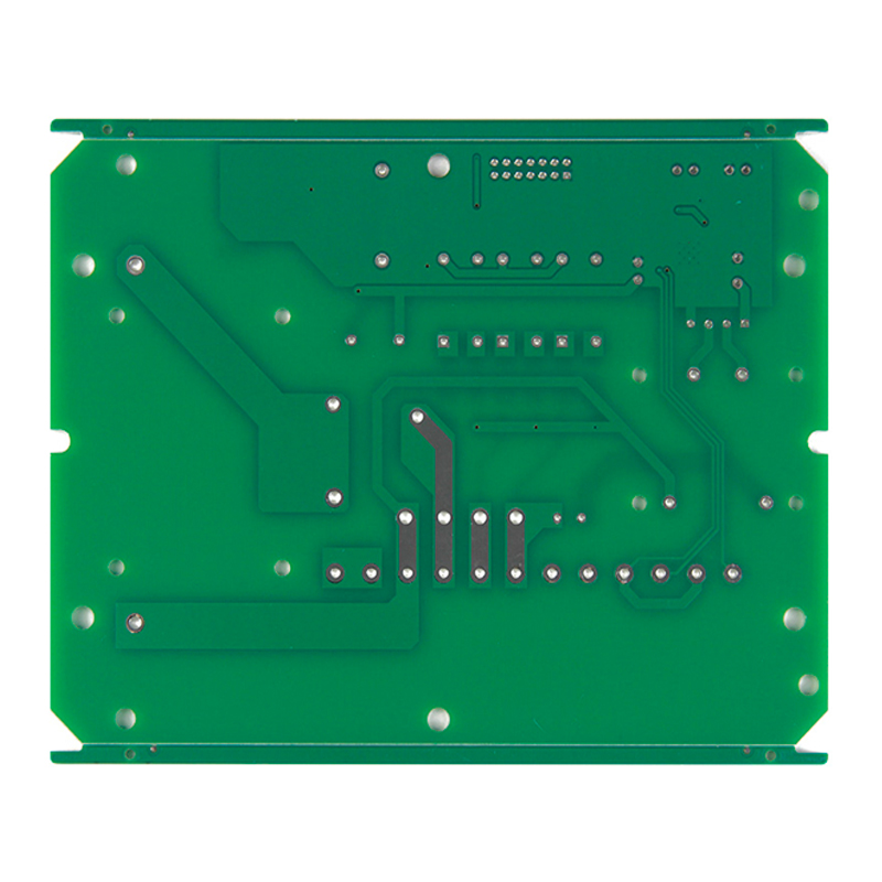
China Professional Custom 94v0 PCB Quick-turn Prototype Printed Circuit Board PCB Express Service Manufacturer
PRODUCT SPECIFICATION:
MANUFACTURING CAPABILITY:
1. Layer Count: 1- 32L
2. Max. Size: 1200 * 600mm
3. Copper thickness: 0.5- 14 OZ
4. PCB thickness: 0.2-5.0mm
5. Min. Line width: 0.075mm/ 3mil
6. Min. Space: 0.075mm/ 3mil
7. Min. Drilling: 0.1mm/ 4mil
8. Min solder mask bridge: 0.1mm/ 4mil
9. Min. Outline tolerance: ±0.10mm/ 4mil
10. Impedance control tolerance: ±10%
11. V slot angel: 30°/ 45°/ 60°
12. Hole size tolerance: ±0.05mm
13. Hole tolerance: ±0.076mm
14. Solder mask type: Sensitive ink
15. Laminate tolerance: 8%; Bend: 0.5%
16. Other test requirements: Dip tin test, tensile test, impedance test
17. Surface finish: HASL (Lead Free), Immersion Tin, Gold Plated, ENIG, OSP, Gold finger, ect.
18. PCB flying probe test, Test jig test
EXPRESS PCB LEAD TIME:
PCB APPLICATION:
PHILIFAST customize varies type of PCB to meet our customers’ requirements.With the rapid and constant development of electronics technology, Printed circuit boards have been widely designed and applied to all kinds of fields to satisfy society demands.
1. Consumer Electronics
2. Medical Devices
3. Industrial electronics
4. Automotive Applications
5. Aerospace facility
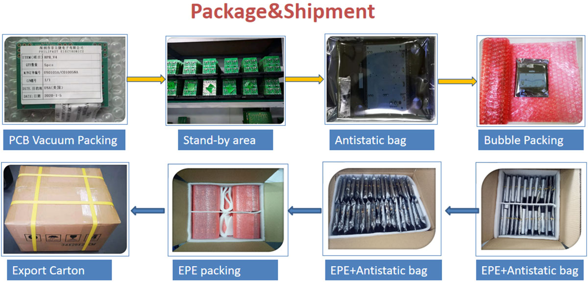
Packing&Shipping:
FAQ:
1,What files are necessary for us to assembly PCBs for you?
1.1 PCB files(Gerber files)
1.2 BOM(Bill of components)
1.3 Cendroid files/Pick&place files)
1.4 Assembly drawings
In order to ensure the quality, BOM files must be clearly noted specific part number,Brand required.it’s very important for us to purchase right components for your project.
2, Lead time for Turnkey circuit board assembly service(small or medium- sized batch)?
2.1 PCB fabrication: Normally 6-15days after engineering query
2.2 Parts: Normally 3-15days (Stocked parts: 3-7days; Imported parts:10- 15days)
2.3 Assembly: Normally 3- 7days (from parts IQC to packing)
2.4 Shipping: Normally 3- 7days (depends on EXPRESS), Forwarder appointed by customer supported.
So, it usually takes around 10- 25days lead time for turnkey PCB assembly.