• facebook
  • linkedin
  • twitter
  • youtube
Untranslated

Big discounting Pcb With Assembly - Shenzhen OEM/ODM Gateway Mainboard PCB Circuit Board Manufacture 1-32 Layers Multi-layer PCB Prototype Manufacturer With Turnkey PCB Service – PhiliFast

Short Description:


Product Detail

Product Tags

Related Video

Feedback (2)

The business keeps to the operation concept "scientific management, premium quality and efficiency primacy, customer supreme for 2 Layer Pcb, Pcb Power, Pcb Circuit Manufacturer, With a wide range, top quality, realistic costs and good company, we are going to be your most effective company partner. We welcome new and aged clients from all walks of daily life to call us for long term small business interactions and acquiring mutual achievements!
Big discounting Pcb With Assembly - Shenzhen OEM/ODM Gateway Mainboard PCB Circuit Board Manufacture 1-32 Layers Multi-layer PCB Prototype Manufacturer With Turnkey PCB Service – PhiliFast Detail:

PRODUCT SPECIFICATION:

Base Material: FR4-TG140 Surface Finish: HASL(Lead Free)
PCB Thickness: 1.6mm Solder Mask: Green
PCB Size: 96*120mm Silkscreen: White
Layer Count: 2/L Cu Thickness 35um(1oz)
Mounting Type: SMT+DIP Application Gateway
Testing Service AOI,X-Ray,Function Test Supplier type Assembly factory

Turnkey Sevices:

1. PCB fabrication

2. Turnkey PCBA: PCB+components+SMT and through-hole assembly+enclosure molding&housing

Main Product:

Gateway PCB

Our Advantage:

1, Programming and Functional test

2, IPC-A-610E standard, E-test, X-ray, AOI test, QC, 100% functional test.

3, Professional service. ISO SMT and through hole assembly, over 10 years experience.

4, Certification: 94v-0, CE, SGS, FCC, RoHS, ISO9001:2008, ISO14001

5, Warranty period for PCBA: 2 years.

PCBA PROCESSING CAPABILITY:

Turnkey PCBA PCB+components sourcing+assembly+package
Assembly details SMT and Thru-hole,PCB enclosure assembly
Lead Time Prototype: 10-12 working days. Mass order: 18~20 working days
Testing on products Flying Probe Test,E-Testing, X-ray Inspection, AOI Test, Functional test
Quantity Min quantity: 1pcs. Prototype, small order, mass order
Files type PCB: Gerber files(CAM, PCB, PCBDOC)
Components: Bill of Materials(BOM list)
Assembly: Pick&Place file, Assembly drawing
PCB Panel Size Min size: 0.25*0.25 inches(6*6mm)
Max size: 20*20 inches(500*500mm)
PCB Solder Type Water Soluble Solder Paste, RoHS lead free
Components details Passive Down to 01005 size
BGA and QFN For Chip
Double-sided SMT Assembly
Fine Pitch to 0.8mils
Part Removal and Replacement
Component package Cut Tape,Tube,Reels,Loose Parts

PCB PROCESSING CAPABILITY:

1

Layers 1-32 Layer
 2 Board material type FR4,Ceramic substrate board,aluminum based board, high-Tg, Rogers and more
 3 Compound material lamination 4 to 6 layers
 4 Maximum dimension 600 x 1200mm
 5 Board thickness coverage 0.2 to 6.00mm
 6 Minimum line width 3mil
7 Minimum line space 3mil
8 Outer layer copper thickness 8.75 to 175µm
9 Inner layer copper thickness 17.5 to 175µm
10 Drilling hole diameter (mechanical drill) 0.25 to 6.00mm
11 Finished hole diameter (mechanical drill) 0.20 to 6.00mm
12 Hole diameter tolerance (mechanical drill) 0.05mm
13 Hole position tolerance (mechanical drill) 0.075mm
14 Laser drill hole size 0.10mm
15 Board thickness and hole diameter ratio 10:1
16 Solder mask type Green, Yellow, Black, Purple, Blue, White and Red
17 Minimum solder mask Ø0.10mm
18 Minimum size of solder mask separation ring 0.05mm
19 Solder mask oil plug hole diameter 0.25 to 0.60mm
20 Impedance control tolerance ±10%
21 Surface finish HASL(Lead Free), ENIG, immersion silver, gold plating, immersion tin and gold finger

Fast Delivery:

PCB In 12Hours
PCBA In 3Days

Main Products Application:
*Medical Products
* Automotive Products
* Industrial Products
* Communication Products(AVL/GPS/GSM Devices)
* Consumer Electronics.

PCB Assembly Procedures:

* Program Management
PCB Files → DCC → Program Organizing → Optimization → Checking
* SMT Management
PCB Loader → Screen Printer → Checking → SMD Placement → Checking → Air Reflow → Vision Inspection → AOI → Keeping
* PCBA Management
THT→Soldering Wave (Manual Welding) → Vision Inspection → ICT → Flash → FCT → Checking → Package → Shipment

PHILIFAST provides you the best PCB manufacture and assembly experience


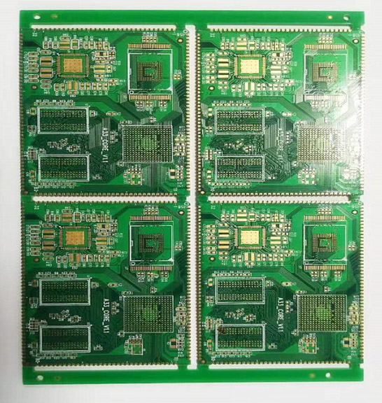
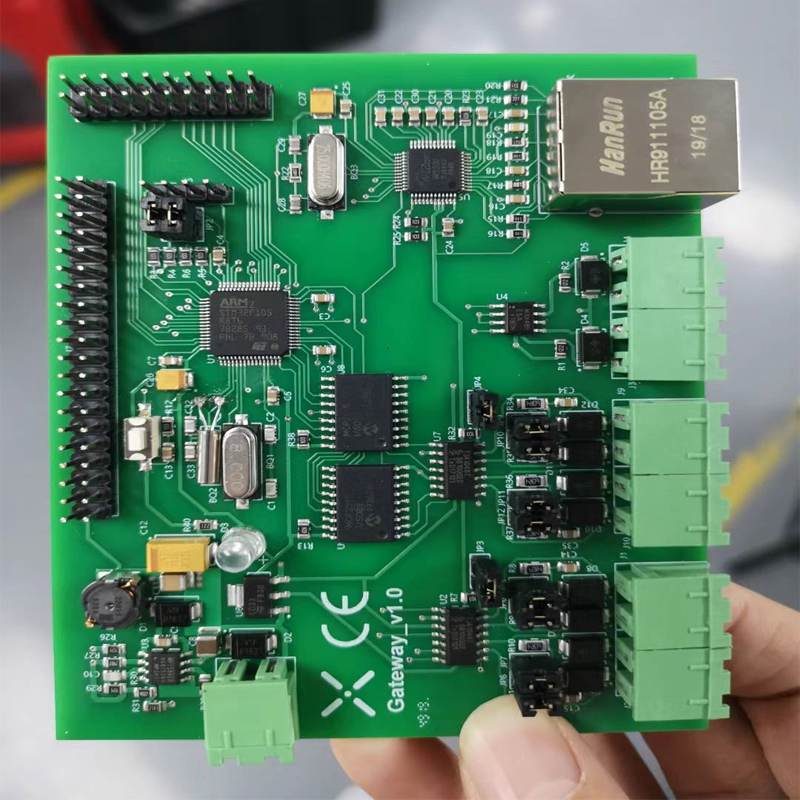
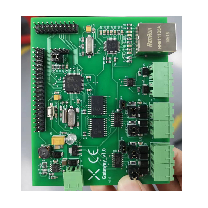
Product detail pictures:

Big discounting Pcb With Assembly - Shenzhen OEM/ODM Gateway Mainboard PCB Circuit Board Manufacture 1-32 Layers Multi-layer PCB Prototype Manufacturer With Turnkey PCB Service –  PhiliFast detail pictures

Big discounting Pcb With Assembly - Shenzhen OEM/ODM Gateway Mainboard PCB Circuit Board Manufacture 1-32 Layers Multi-layer PCB Prototype Manufacturer With Turnkey PCB Service –  PhiliFast detail pictures


Related Product Guide:

While using the "Client-Oriented" organization philosophy, a rigorous top quality command process, highly developed production devices and a potent R&D workforce, we normally provide high quality products, outstanding solutions and aggressive charges for Big discounting Pcb With Assembly - Shenzhen OEM/ODM Gateway Mainboard PCB Circuit Board Manufacture 1-32 Layers Multi-layer PCB Prototype Manufacturer With Turnkey PCB Service – PhiliFast, The product will supply to all over the world, such as: Colombia, Chile, Lahore, We only supply quality items and we believe this is the only way to keep business continue. We can supply custom service too such as Logo, custom size, or custom merchandise etc that can according to customer's requirement.
  • The supplier cooperation attitude is very good, encountered various problems, always willing to cooperate with us, to us as the real God.
    5 Stars By trameka milhouse from Seychelles - 2018.12.28 15:18
    The company can think what our think, the urgency of urgency to act in the interests of our position, can be said this is a responsible company, we had a happy cooperation!
    5 Stars By Mignon from Suriname - 2018.12.11 11:26
    Write your message here and send it to us

    Related Products

    top