Realiable Oem Electronic Pcb Manufacturing Multilayer Pcb Circuit Board Fabrication Assembly Manufacturer Gold Plated Pcb Board Production


PRODUCT SPECIFICATION:
| Base Material: | FR4-TG140 | Surface Finish: | ENIG |
| PCB Thickness: | 1.6mm | Solder Mask: | Blue |
| PCB Size: | 86*135mm | Silkscreen: | White |
| Layer Count: | 2/L | Cu Thickness | 35um(1oz) |
To ensure an accurate quote, be sure to include the following information for your project:
•Complete GERBER files including the BOM list
•Other file types (Altium,Protel,OrCAD)
•"Read Me" notes for additional fabrication information
•Quantities
•Turn time
•Panelization Requirements
•Materials Requirements
•Finish requirements
Your custom quote will be delivered in just 2-24 hours, depending on the design complexity.
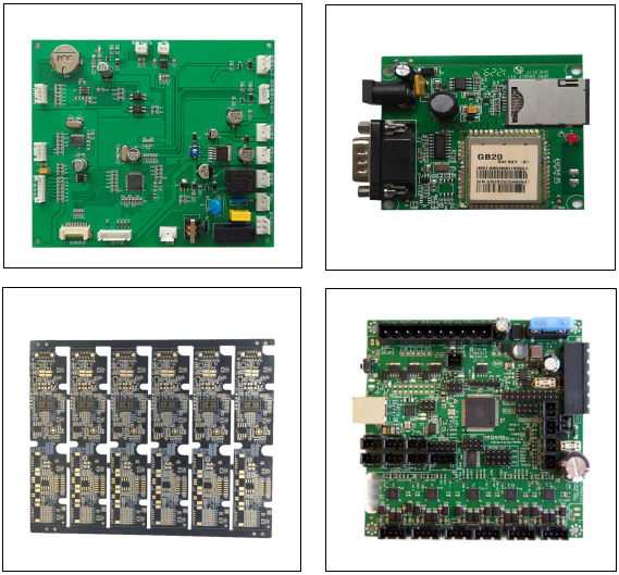
OEM Finished product assembly
1. One-step service
2. Can be customized according to customer requirements packaging equipment.
3. Processing of semi-finished products
4. Finished product assembly
5.Check completed
6.Shipping
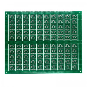
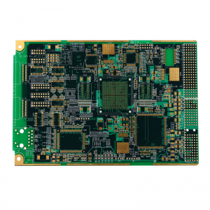
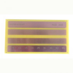
Main Product:
Our Capability:
| Product Name | Module PCB |
| Type | Rigid PCB |
| Material | FR4, Aluminum,Copper,Rogers, PI, PET, ect... |
| Layer | 1,2,4,6...32Layer |
| Shape | Rectangular, Round, Slots, Cutouts, Complex, Irregular |
| Cutting | Shear, V-score, Tab-routed |
| Board Thickness | 0.2-4mm, regular 1.6mm |
| Copper Thickness | 0.5-4oz, regular 1oz |
| Solder Mask | Green,Matt Green, Black, Matt black, Red, Blue, Yellow, etc. |
| Silk Screen | White, Black, etc. |
| Silk Screen Min Line Width | 0.006" or 0.15mm |
| Min Trace/Gap | 0.1mm or 4mils |
| Min Drill Hole Diameter | 0.01",0.25mm or 10mils |
| Surface Finish | HASL, ENIG, OSP, etc. |
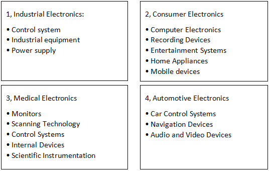
APPLICATION FIELD:
PCB are customized as per customer’s design files,widely used in automotive electronics, communications industry, industrial control, medical, power and energy, LED lighting, solar panels, safety monitoring and semiconductor fields.
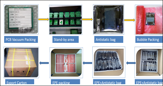
Package&Shipment:
1,For small order,We usually use EXPRESS shipping to ensure the timely delivery.such as FedEx, DHL, UPS, TNT, EMS, private lines, etc., those Express has better time effect,and won’t damage the goods. All shipping will be in time without too much delay.
2,For mass production,We usually use Sea shipping to save your cost.
3,Also, If you can appoint your own forwarder, we can ship the goods to your own carrier.
RFQ:
1: What files do we accept?
DXP,Protel99, CAM, Gerber,...
2: Do you keep our files confidential
We customize PCBs as per customer’s design files, all files from customers are strictly confidential, and we sign Non-Disclosure Agreement
3: How do you pack your PCBs?
We packed our products as below: